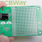
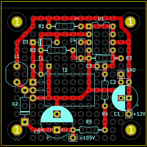
General principle from YouTube video for a small prototype board. In addition to an array of holes, can add power elements, standard items, etc.
- In KiCAD add footprint “1X01_NO_SILK” currently in LFO folder “_parts”; this adds a single plated through hole
- With single footprint, right-click and select “Footprint Properties”
- IMPORTANT: Tick “Not in schematic” to ensure any updates from the schematic do not delete the prototype area
- Switch off “Reference designator” and “Value”, untick “Show” to remove unnecessary items on screen
- Right-click on pad and select “Special Tools” -> “Create Array…”
- Select required number of row and columns. Easier to have too many and delete, than add extras. Ensure spacing is 2.54mm (0.1″)
- Add Net: To add a track connection the pad needs to have a Net name assigned. Right-click -> Properties and add the net, e.g. GND. Can then add track as per normal
- Can add silkscreen boxes around power distribution and add annotations too
KiCAD can also be used for layout on prototype boards:
- Draw a board outline as needed
- Place any mounting holes in their respective places
- Draw a small circle to represent a ‘pad’, or stripes etc
- For grid ‘pads’ 0.762 mm diameter with 0.508 line thickness work well
you only need one circle - Set colour (eg: User.Eco1) and opacity (select circle, and shift-[ or shift-] to set)
- Use Special Tools -> Create Array to layout the rest
- Lock the “holes” afterward to prevent being moved / deleted
- Layout tracks as required to reflect wiring links to be made:


